Why PEEK Is the Preferred Plastic for Semiconductor Equipment Components
PEEK (Polyether Ether Ketone) is one of the most widely used high-performance engineering plastics in semiconductor manufacturing. Known for its exceptional combination of mechanical strength, thermal stability, chemical resistance, and dimensional accuracy, PEEK has become a preferred material for critical components in semiconductor equipment operating in demanding cleanroom environments.
As a semi-crystalline thermoplastic, PEEK delivers outstanding performance across a broad temperature range while maintaining structural integrity under continuous mechanical and chemical exposure. Its low outgassing characteristics, minimal particle generation, and high purity make it particularly suitable for contamination-sensitive semiconductor processes.
Compared with conventional engineering plastics, PEEK offers significantly better dimensional stability, wear resistance, and long-term reliability. These characteristics have made it a standard material for precision components used throughout wafer handling, process equipment, inspection systems, and semiconductor testing applications.
Key Material Properties of PEEK
PEEK combines multiple performance advantages that are difficult to achieve with other engineering plastics:
Exceptional Mechanical Strength
PEEK maintains high tensile strength, stiffness, and impact resistance, even under continuous loading conditions. Its excellent fatigue resistance allows components to withstand repeated mechanical cycles without significant degradation.
High Temperature Resistance
PEEK can operate continuously at temperatures up to approximately 250°C while retaining its mechanical properties. This makes it ideal for semiconductor equipment exposed to elevated process temperatures.
Outstanding Chemical Resistance
The material resists a wide range of aggressive chemicals, acids, solvents, and cleaning agents commonly used in semiconductor manufacturing environments.
Low Outgassing and Low Particle Generation
For cleanroom applications, material cleanliness is critical. PEEK exhibits extremely low outgassing and particle shedding, helping reduce contamination risks during wafer processing.
Excellent Dimensional Stability
PEEK exhibits minimal thermal expansion and maintains tight dimensional tolerances across varying operating conditions, meeting the precision requirements of semiconductor equipment.
Electrical Insulation Performance
Its high dielectric strength and electrical insulation properties make PEEK suitable for components operating near sensitive electronic systems.
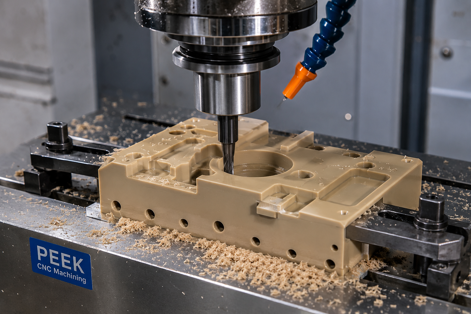
CNC Machining Challenges of PEEK
Although PEEK offers excellent performance advantages, it presents several unique challenges during precision CNC machining.
1. High Cutting Forces and Tool Wear
PEEK combines high strength with exceptional toughness. During machining, cutting forces can be substantial, requiring rigid machine platforms and optimized machining strategies.
Standard tooling often experiences rapid wear or edge chipping when machining PEEK. For consistent performance, specialized carbide cutting tools are typically required to maintain surface quality and dimensional accuracy.
2. Heat Buildup During Machining
Unlike metals with high thermal conductivity, PEEK tends to retain heat in the cutting zone. Excessive heat accumulation can lead to:
● Material softening
● Edge burr formation
● Surface discoloration
● Localized thermal deformation
● Dimensional inaccuracies
Effective heat management is essential for maintaining precision tolerances and preventing material damage.
3. Internal Stress and Post-Machining Deformation
As a semi-crystalline polymer, PEEK can develop residual stress during machining operations. If not properly controlled, these stresses may cause warping or dimensional changes after machining, especially in high-precision semiconductor components.
Stress-relief processes and optimized machining sequences are often necessary to ensure long-term dimensional stability.
4. Complex Geometry Machining
Many semiconductor components incorporate:
● Thin-wall structures
● Deep pockets
● Micro-holes
● Precision grooves
● Complex geometries
These features increase the risk of edge chipping, cracking, or dimensional instability, requiring specialized machining expertise and process control.
Common Semiconductor Applications for CNC-Machined PEEK Components
PEEK plays a critical role throughout semiconductor manufacturing equipment due to its combination of cleanliness, precision, and durability.
Wafer Handling Components
PEEK is widely used in:
● Wafer carriers
● Wafer guides
● Wafer retaining rings
● End effectors
● Transfer mechanisms
These components require excellent dimensional accuracy and minimal particle generation during operation.
Vacuum and Process Fixtures
The material is commonly selected for:
● Vacuum chuck components
● Vacuum suction fixtures
● Precision positioning fixtures
● Semiconductor tooling systems
Its dimensional stability and low outgassing characteristics make it highly suitable for vacuum environments.
Etching and Process Equipment Components
PEEK components are frequently found in semiconductor process equipment where resistance to aggressive chemicals and elevated temperatures is required.
Test and Inspection Systems
Applications include:
● High-temperature test sockets
● Precision inspection fixtures
● Alignment components
● Probe support structures
The material's electrical insulation and thermal stability provide reliable performance during testing operations.
Packaging and Back-End Equipment
PEEK is increasingly used in semiconductor packaging and testing equipment, where precision, cleanliness, and wear resistance are essential for maintaining production efficiency and yield.
By minimizing contamination risks and maintaining stable performance under demanding operating conditions, PEEK directly improves process reliability and manufacturing yields.
Precision PEEK CNC Machining Services from 3DPanther
3DPanther provides precision CNC machining services for PEEK and other high-performance engineering plastics used in semiconductor, electronics, medical, and industrial applications. Leveraging advanced CNC equipment, specialized tooling, and extensive machining expertise, we produce complex PEEK components with tight tolerances up to ±0.005 mm. From prototypes to production runs, we deliver reliable, high-quality parts that meet demanding requirements for precision, cleanliness, and long-term performance.